• India’s #1University (2016-23) & Research Institute (2021-23)*
  • 4 Days Campus
    Visit
  • 100% Live Interactive
    Classes
  • 9 Months
    Programme
  • *As per NIRF Ranking 2023

Massive Growth Opportunity

  • With chip demand set to rise over the coming decade at 7% CAGR, the global semiconductor industry is poised to become a trillion-dollar industry by 2030, driven by the automotive, data storage, and wireless industries.1
  • India's Semiconductor market will touch $64 billion by 2026 almost three time its 2019 size of $22.7 billion.2 - Report by Counterpoint Research and the IESA
  • India's semiconductor consumption will be the highest in the world, worth $110 billion by 2030.3-MoS, IT

4 Reasons Why This Programme is Unique

1 Get the IISc Advantage

  • Designed by IISc’s Department of Electronics Systems Engineering
  • Delivered by top researchers in VLSI Design and Application
  • Access to the VLSI Research Labs to implement projects
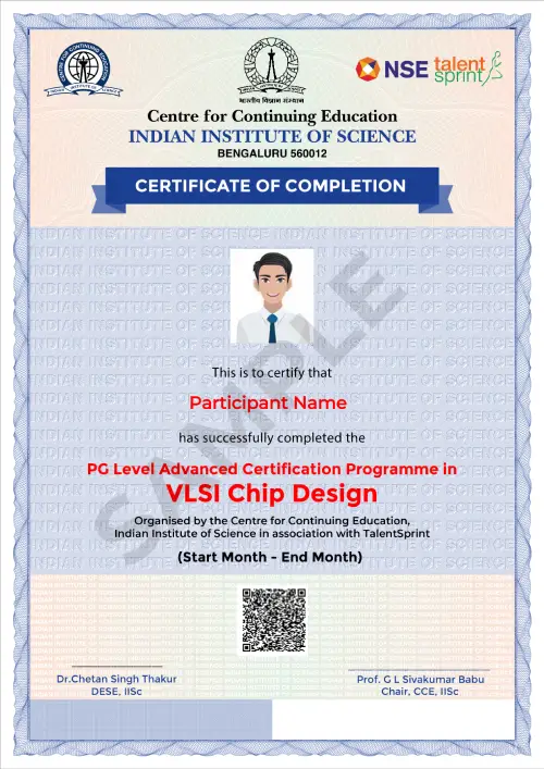
  • Get globally recognized certificate from Center for Continuing Education at IISc

2 Cutting-edge Applied Learning

  • Practise on FPGA Boards
    and Cadence Tools
  • Hands on curriculum for effective
    learning by practitioners
  • Opportunity to implement your projects
    in state of art research labs
  • Industry interactions with
    VLSI leaders

3 Career Impact

  • Showcase your expertise through
    projects and experiments
  • Network with future leaders
    of chip design
  • Upgrade your technical profile
    with a top certification

4 Get TalentSprint Advantage

  • Learn on TalentSprint’s patent-pending Digital Platform
  • Network with 3000+ TalentSprint
    Deep Tech Alumni
  • Access TalentSprint
    Career Accelerator

Curriculum

  • CMOS standard cell characteristics
  • Delay calculation (Elmore model, Logical Effort)
  • Low power design
  • Static Timing Analysis
  • Digital ASIC design flow

  • Device Physics of the MOSFET
  • Physics Insights: MOSFET as a Switch
  • Analytical Techniques: Low and High frequency analysis, Noise analysis
  • Feedback
  • OPAMP Design
  • Oscillators and Phase Locked Loops
  • Analog Integrated Circuits Beyond Silicon

  • Open Source Processor Architecture (RISC-V)
  • Neuromorphic Computing
  • Edge Computing
  • Flexible Electronics

  • VLSI Micro-architecture Design
  • Timing Closure
  • High Throughput Computing
  • FPGA Based System Design
  • Processor Design

Projects

  • Machine Learning Accelerator
    for Image Classification Task
  • Datapath and
    Controller Design
  • And More...

Apply Now

Download Brochure

Tools

  • Cadence Analog
    Design Tool Suit
  • Xilinx
    Vivado
  • BASYS3 FPGA Board
    with Pmods
  • Digital VLSI
    Design Tool Suit

Lab Exercises

  • Operation Amplifier
    Design
  • ASIC Design
    Flow
  • Transient Analysis of
    Standard Cells
  • Combinational, Sequential
    Circuit Design
  • Algorithm to
    Architecture
  • Design with
    FPGA Boards

Schedule

  • 9 Months Executive friendly programme IISc faculty members-led Live interactive classes, capstone projects, industry sessions and campus visits to IISc
  • 204 hours of immersive learning, including live classes, mentored-assisted hands-on sessions, Capstone Projects, campus visits and industry sessions
  • Participants will have two campus visits of 2 days each
  • Classes will be held every weekend for 2-3 hours

Eligibility

  • Education: B.E./M.E./B.Tech/M.Tech or an equivalent degree
  • Experience: Minimum 1 Year
  • Exposure: Working in VLSI domain or having VLSI working knowledge

What is My Investment?

Application Fee
₹2,000


Total Programme Fees ₹2,80,000
Program Fee with Scholarship ₹2,10,000
Programme Kit (Extra*)
(FPGA Boards with Cadence Tools) ₹75,000
(18% GST extra as applicable)


Special Pricing for Corporates

Fees paid are non-refundable and non-transferable.

Modes of payment available

  • Internet Banking
  • Credit/Debit Card
  • UPI Payments

Easy Financing Options

12 Month 0% Interest Scheme / Interest-Based Schemes

Financing as low as ₹9,530/Month*

EMI Options

Loan Partners

Programme Kit (Extra*)

Programme Fee for International Participants $4,150
With Scholarship $3,100

Programme Kit
(FPGA Boards with Cadence Tools)

$1,000