Design the chip of the Future
Advanced Certification Programme in VLSI Chip Design
VLSI Course for Working Professionals, offered by
TalentSprint in collaboration with CCE at IISc

Design the chip of the Future
Advanced Certification Programme in VLSI Chip Design
The Advanced Certification course in VLSI Chip Design offered by TalentSprint in collaboration with CCE at IISc, enables professionals to build VLSI chip designing capabilities that can power new-age technologies like AI, IoT, VR, Mobility, Cloud, and Analytics.
VLSI, along with embedded software development and hardware/board design, is at the heart of the chip design industry. With the global semiconductor industry projected to become a trillion-dollar industry by 2030, there is a need to design and produce highly efficient and specialised chips.
The Department of Electronic Systems Engineering, with its pioneering and ongoing research and training in VLSI chip design, is best positioned to offer this programme . The programme is ideal for VLSI industry professionals who want to leverage expertise of modern tools and technologies.
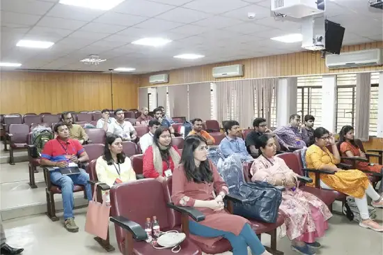
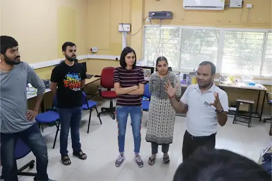
The 9-month course is delivered in a unique experiential learning process of interactive online sessions by IISc faculty members, starting from essential theoretical foundations to learning how to apply them in the real world effectively. This is accompanied by laboratory exercises using VLSI tools and boards, mentor support, case studies, and 4 days of IISc campus visit to ensure fast-track learning.

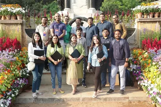
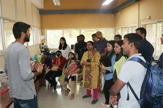
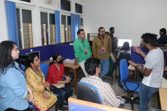
IISc Campus Visit


The Advanced Certification Course in VLSI Chip Design is offered by TalentSprint in collaboration with CCE at IISc.
Department of Electronic Systems Engineering (DESE). Previously known as the Centre for Electronics Design and Technology (CEDT) it was started with support from the Department of Electronics (DoE), University Grants Commission (UGC), and Swiss Development Cooperation (SDC). DESE aims to achieve excellence in research and education in electronics systems engineering, with positive societal impact. For more information, visit https://www.iisc.ac.in
IISc is India’s premier institution for advanced scientific and technological research and education.IISc’s reputation and pre-eminence attract the finest academicians trained in the best laboratories around the world. In 2018, IISc was selected as an Institution of Eminence (IoE) by the Government of India, and it consistently figures among the top Indian institutions in world university rankings. The alumni of IISc hold significant academic and industry positions around the globe. For more information, visit, https://dese.iisc.ac.in/.
Learn from a dynamic IISc faculty members, all with academic and research credentials from esteemed educational institutions.
Programme Director
 Dr. Chetan Singh
 Ph.D., Neuromorphic Engineering, MARCS Research Institute, Western Sydney University, Australia
Research Expertise: Neuromorphic Computing, Mixed Signal VLSI Systems, Analog/Digital ASIC design
PROGRAMME FACULTY
 Kuruvilla
 Research Expertise: Digital Systems, VLSI, High Performance Accelerators, Computer Networks
PROGRAMME FACULTY
 Dr. Sanjiv
 Ph.D., Electrical and Computer Engineering, University of Waterloo, Canada
Research Expertise: Semiconductor Physics, Flexible Electronics
PROGRAMME FACULTY
 Dr. Arup
 Ph.D., Electrical and Computer Engineering, Georgia Tech, USA
Research Expertise: Analog and Mixed Signal Design, Multi-Mode Fiber Systems
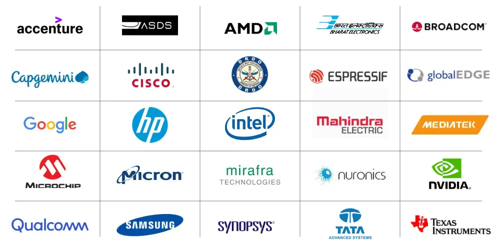
All logos belongs to respective companies
Note: These are edited versions based on the details submitted by various programme applicants.
It's a simple 4-step process
Application Fee*
₹2,000
Total Programme Fees* ₹2,80,000
Program Fee with Scholarship ₹2,10,000
Programme Kit (Extra*)
(FPGA Boards with Cadence Tools) ₹75,000
(*18% GST extra as applicable)
*Fees paid are non-refundable and non-transferable.
![]() Special Pricing for Corporates **
Special Pricing for Corporates **
**Applicable only for enterprises nominating their employees as a group
Modes of payment available
 Internet Banking
 Credit/Debit Card
 UPI Payments
Financing as low as ₹12,074/Month*
Loan Partners


Programme Kit (Extra*)
| Programme Fee for International Participants | $4,150 |
| With Scholarship | $3,100 |
Programme Kit (FPGA Boards with Cadence Tools) |
$1,000 |
VLSI, along with embedded software development, and hardware/board design is at the heart of the chip design industry. It is an integral part of the Electronic Systems Design and Manufacturing (ESDM) sector.
Some of the important developments listed here indicate that the sector is transforming lives, businesses, and economies across the world.
This is the right time for current and aspiring VLSI professionals and entrepreneurs to invest in building expertise and tap into the promising opportunities that this sector offers.
TalentSprint has partnered with Center for Continuing Education (CCE) at IISc for their executive education programmes in disruptive and emerging technologies.
IISc is India's premier institution for advanced scientific and technological research and education. It is one of the first three publicly funded institutes to be awarded the Institute of Eminence status.
The institution's reputation and pre-eminence consistently feature it in global university rankings. The institution has been home to distinguished alumni who have had noteworthy academic and industry positions around the globe.
IISc has been consistently recognised as India’s #1 Research Institute (2021-24) & #1 University (2016-24) by the National Institutional Ranking Framework (NIRF) 2024 Ranking. For More information, visit https://www.nirfindia.org/Rankings/2024/Ranking.html
TalentSprint brings high-end and deep-tech education to aspiring and experienced professionals in partnership with top academic institutions and global corporations. Its patent-pending, AI-powered, digital learning platform enables a perfect blend of high-end academics and industry-leading practitioner experience. TalentSprint offers in-depth understanding of the deep technologies, access to industry experts, and a state of art technology platform. To know more visit www.talentsprint.com.
The VLSI field is highly technical, and there are massive opportunities in the semiconductor industries for professionals with desired expertise. Some specialized roles in VLSI that tech professionals can transition to are,
Get CCE-IISc Advantage
Cutting-edge Applied Learning
Career Impact
TalentSprint Advantage
